ISO 9001:2015 CERTIFIED (No. 29024010637-03R0S) Shenzhen Factory: ONLINE (2h Rapid DFM Response Guarantee)
HIGH-TECH & SEMI • SILICON PROCESSING

Wafer Handling & Lids

Zero-Particle PEEK End-Effectors & Front-Opening Unified Pod (FOUP) Lids.

Ultra-precision machined static-dissipative Semitron, virgin PEEK 450G, and Teflon wafer end-effector vacuum wands, cassette carrier doors, and CMP retaining rings engineered for damage-free handling of 200mm and 300mm silicon wafers.

ESD Static Dissipative 10⁶–10⁹ Ω
Zero Particle Generation
No Metallic Contamination

Specialized Engineering for Wafer Handling & Lids

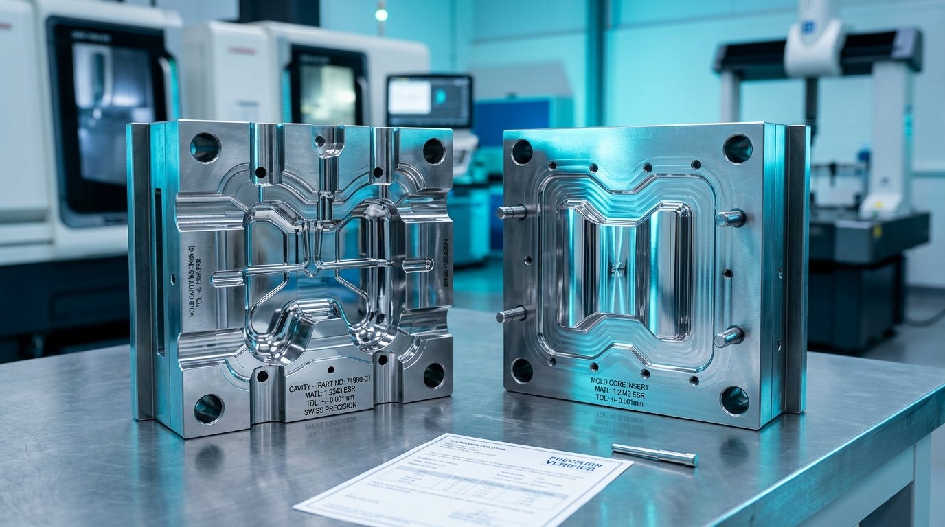
JYH Prototype combines 5-axis CNC machining, micro-tolerance wire EDM, cleanroom injection molding, and Zeiss CMM metrology to supply mission-critical components that meet strict aerospace, medical, automotive, and semiconductor quality benchmarks.

Strict Certifications

AS9100D, ISO 13485:2016, and IATF 16949 certified quality management systems with full lot traceability.

Rapid Turnaround

Fast-track prototyping dispatched in 3–5 business days; production bridge pilot runs ready in 10–14 days.

Advanced Materials

Machining Ti-6Al-4V, Inconel 718, PEEK, Delrin, Al 7075-T651, Kovar, and OFHC Ultra-pure Copper.

100% CMM FAI Reports

Zeiss 3D CMM inspection, optical laser profilometry, and AS9102 Form 3 FAI dimensional verification.

Technical Deep Dives: Wafer Handling & Lids

Four critical manufacturing challenges solved by our Shenzhen engineering team through advanced tooling, multi-axis kinematics, and rigorous quality assurance.

Semitron ESd 225 & PEEK Wafer Wand End-Effectors 500 × 500 HD Natural

Semitron ESd 225 & PEEK Wafer Wand End-Effectors

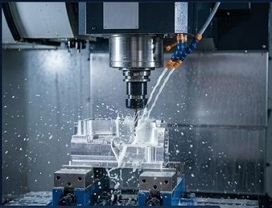
Micro-milling ultra-thin vacuum pick-up wands with integrated vacuum suction holes (0.3mm) for robot arms loading 300mm wafers.

  • Machined with calibrated multi-axis toolpaths minimizing tool deflection
  • GD&T true position inspected within ±0.005mm using automated CMM
  • Full material mill certs, heat treat data, and FAI documentation provided
Request Quotation for Similar Geometry
Chemical Mechanical Planarization (CMP) Retaining Rings 500 × 500 HD Natural

Chemical Mechanical Planarization (CMP) Retaining Rings

Precision turning and slotting of PPS and PEEK rings holding wafers flat against polishing pads under chemical slurry exposure.

  • Machined with calibrated multi-axis toolpaths minimizing tool deflection
  • GD&T true position inspected within ±0.005mm using automated CMM
  • Full material mill certs, heat treat data, and FAI documentation provided
Request Quotation for Similar Geometry
FOUP Cassette Door Hermetic Precision Lids 500 × 500 HD Natural

FOUP Cassette Door Hermetic Precision Lids

Lightweight carbon-fiber filled polyetherimide (Ultem) lids with perimeter seal grooves protecting wafers from airborne ambient particles.

  • Machined with calibrated multi-axis toolpaths minimizing tool deflection
  • GD&T true position inspected within ±0.005mm using automated CMM
  • Full material mill certs, heat treat data, and FAI documentation provided
Request Quotation for Similar Geometry
Non-Contact Optical CMM Contour Validation 500 × 500 HD Natural

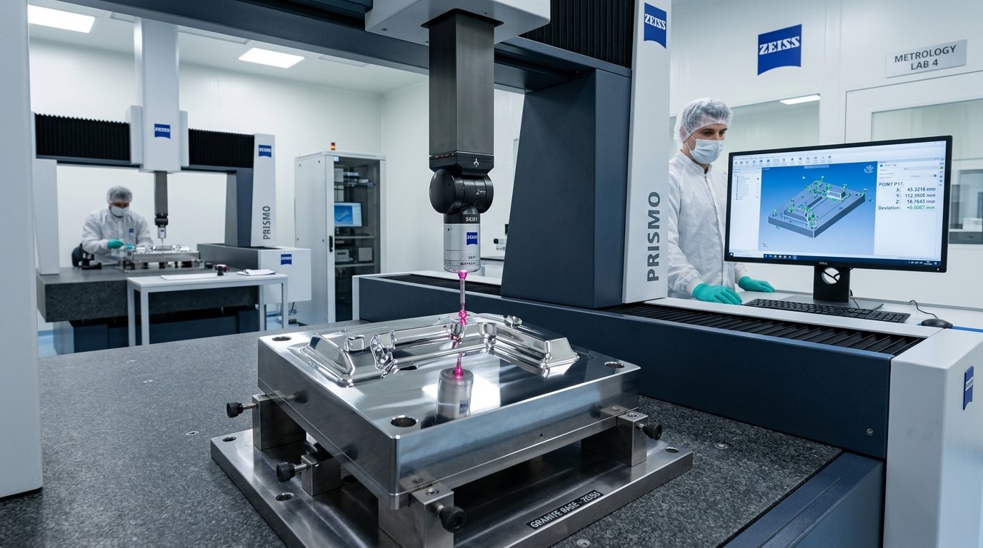
Non-Contact Optical CMM Contour Validation

Multi-sensor laser scanning of wafer contact lands ensuring zero contact stress concentrations that could micro-crack silicon dies.

  • Machined with calibrated multi-axis toolpaths minimizing tool deflection
  • GD&T true position inspected within ±0.005mm using automated CMM
  • Full material mill certs, heat treat data, and FAI documentation provided

Request Quotation for Similar Geometry

Capabilities & Quality Protocols

Every part manufactured at JYH Prototype adheres to international engineering standards and rigorous metrology protocols.

Machining & Tooling Capabilities

  • Machining of Advanced Semiconductor Engineering Plastics
  • Cryogenic De-Burring of Micro-Features
  • ESD Surface Resistivity Verification Testing
  • Class 100 Cleanroom Double-Bagged Packaging

Metrology & Quality Assurance

  • Zeiss PRISMO 3D CMM Metrology with scanning resolution down to 0.9µm
  • Keyence Optical Non-Contact Flash Measuring System for micro-features
  • XRF Spectrometry for raw metal alloy composition verification
  • AS9102 Form 1, Form 2, and Form 3 First Article Inspection (FAI) packages

Ready to Prototype or Scale Wafer Handling & Lids?

Upload your 3D CAD models (.STEP, .IGES, .SLDPRT, .X_T) or 2D technical drawings (.PDF, .DWG) to receive an interactive quote with comprehensive Design for Manufacturability (DFM) feedback in under 2 hours.

Upload CAD Files Now
💬

Connect on WeChat

Scan the QR code or search WeChat ID to speak directly with our Shenzhen engineering team.

WeChat ID: JYH-Prototype
JYH AI Assistant · 智能客服
Online 24/7 · 全天在线
Get Instant Quote
Shenzhen High-Tech Industrial Park
+86 137 1457 8126